Scope note. This article states only conclusions supported by GB202 runtime experiments, driver objects, and firmware code. Any on-die topology that the available evidence cannot determine is explicitly marked as inference or unknown.
Public NVIDIA overclocking interfaces normally expose only core clock, memory clock, voltage, and the power limit. XBAR is rarely shown at all, making it easy to mistake for a software statistic, a derivative of core frequency, or an internal name with no useful control surface. None of those explanations holds on the RTX 5090's GB202. XBARCLK has its own PMU object, clock source, V/F-point state, hardware frequency-measurement entry point, and runtime control. Changing it changes both the physically measured clock and real rendering throughput. It is neither an alias for GPCCLK nor another notation for MCLK; it is a physical clock domain that participates in voltage, power, and cross-domain clock arbitration.
Calling it a “physical clock domain” does not mean that the exact boundary of one box on the die floorplan is known. The evidence establishes that a set of independently firmware-managed hardware logic uses XBARCLK, with an independent clock source and register-programming path, and that under load it affects throughput through the GPU's internal data path. The name XBAR naturally suggests a crossbar or on-chip interconnect, but a name plus performance behavior is not enough to identify every connected cache, partition, or controller. This article therefore uses “the XBAR physical clock domain” without inventing a GB202 interconnect diagram that NVIDIA has not published.
Why XBARCLK is not a subordinate GPCCLK reading
The active clock-domain table in the current GB202 PMU image contains all of the following objects:
| Domain | mask | PMU object | local source ID |
|---|---|---|---|
| GPCCLK | 0x00000001 |
0x200ed398 |
3,4,5,6,7,8,12,13 |
| XBARCLK | 0x00000002 |
0x200ed4f0 |
2 |
| SYSCLK | 0x00000004 |
0x200ed498 |
— |
| MCLK | 0x00000010 |
0x200ed5a0 |
— |
| XBAR2CLK | 0x00040000 |
0x200ed718 |
— |
GPCCLK and XBARCLK differ not only in object address but also in top-level apply and commit dispatch and in their internal state. The downstream local programming chain for XBARCLK can be closed as follows:
clock request
  -> XBARCLK object apply/commit
  -> common clock-source class, source ID 2
  -> per-source descriptor at PMU DMEM 0x2007d860
  -> div/mux control-word packing
  -> PMU MMIO-window write
This rules out the claim that XBAR is merely a value calculated by the driver from GPCCLK. Firmware really does select and commit independent clock-source parameters for XBARCLK and ultimately sends them through a hardware-register write path. What remains missing is the exact register offset stored in the live descriptor after initialization, not evidence that a hardware write exists.
A second domain named XBAR2CLK exists alongside XBARCLK, but its apply/commit methods in the current PMU image only return status and do not enter the same local hardware-programming chain. XBAR2CLK is therefore more likely to be a logical or API aggregation domain used by the 2X policy, while XBARCLK is the locally programmed physical object. That interpretation is supported by object behavior but remains an inference; similar names are not enough to merge the two domains.
XBAR is controllable, and how the control actually works
“Controllable” here is not inferred from an overclocking UI. R610's private ClockClient exposes domain information, domain control, and independent hardware frequency measurement. The four RM controls used in this work are:
| Operation | command | R610.57.04 parameter size | Purpose |
|---|---|---|---|
CLK_CLK_DOMAINS_GET_INFO |
0x20809019 |
0x3030 |
Obtain active/controllable clock domains and offset ranges |
CLK_CLK_DOMAINS_GET_CONTROL |
0x2080901b |
0x083c |
Read the current domain-control object |
CLK_CLK_DOMAINS_SET_CONTROL |
0x2080d01c |
0x083c |
Submit the complete domain-control object |
CLK_MEASURE_FREQ |
0x20809006 |
0x0008 |
Measure a specified physical clock domain with hardware counters |
In the R610.57.04 0x83c control block verified on hardware:
+0x04  controllable-domain mask; 0x000000ff on this machine

domain header = 0x3c bytes
domain stride = 0x40 bytes
XBAR domain index = 1
XBAR domain base = 0x3c + 1 * 0x40 = 0x7c

+0x84  XBAR frequency-offset mode, i.e. XBAR base + 0x08
+0x88  signed XBAR frequency offset in kHz
+0x90  signed rail-1/MSVDD offset in µV
+0x90 is not a “physical-voltage register” that happens to sit beside the XBAR frequency field. Beginning at +0x8c, the domain record stores requests indexed by voltage-rail number. MSVDD is rail index 1 on this machine, so its location is XBAR base + 0x10 + 1 × 4 = 0x90. The value written there is an XBAR-domain voltage-offset request submitted to the shared-MSVDD arbiter, not an output forced directly into the regulator behind the GSP's back.
A complete, verifiable, and reversible control flow should be:
- Check the parameter size of each command against the target driver's method table or another version description already verified on that exact build. If the size is unknown or mismatched, refuse the write rather than guessing the layout from a version string.
- Call
GET_INFOand verify the active-domain mask, the identity of the XBAR domain, and the offset range returned by the driver. - Call
GET_CONTROLand preserve the entire original control block, not only the four or eight bytes that will be changed. - In a copy of that block, enable XBAR frequency-offset mode and write a signed kHz offset. If needed, also write the XBAR domain's signed MSVDD offset in µV.
- Submit the complete block through
SET_CONTROL. - Call
GET_CONTROLagain and confirm that the driver retained the requested values. - Use
CLK_MEASURE_FREQwith domain mask0x2to read physical XBARCLK instead of presenting readback as if it were an actual frequency. - Measure workload output at the same time. Only a change in both physical clock and useful throughput shows that the request became effective hardware control.
- At the end of the experiment, or on a signal that can be handled safely, write back the entire block saved in step 3, then read and verify the restored values.
The nominal XBAR frequency-offset range returned on this machine is -1000 to +1000 MHz. This is only the range of requests the driver reports as acceptable. It is not a stable range for this sample under every load, and it is not a recommendation to run +1000 MHz daily.
Minimal runnable example
The project's xbar_clock_demo.c is a minimal proof program written for the fixed R610.57.04 layout. It does not try to be a cross-version library. With no arguments it only reads the current XBAR offset and physical frequency. With three arguments it saves the control block, writes the request, reads it back, measures frequency every 100 ms, and restores the original state at the end.
Build:
cc -std=gnu11 -O2 -Wall -Wextra -Wpedantic -Werror \
  xbar_clock_demo.c -o xbar_clock_demo
Read the current state only:
sudo ./xbar_clock_demo
Temporarily request XBAR +60 MHz with 0 µV voltage offset, keep it for two seconds, then restore:
sudo ./xbar_clock_demo 60000 0 2
One measured run produced:
before:  xbar_offset_khz=0 measured_xbar_khz=1439616
readback: xbar_offset_khz=60000 measured_xbar_khz=1462144
restored: xbar_offset_khz=0 measured_xbar_khz=1440061
The argument sequence for simultaneously requesting XBAR +450 MHz and an XBAR-domain MSVDD offset of +20 mV is:
sudo ./xbar_clock_demo 450000 20000 2
The same program retains the control entries used to separate XBAR effects from SYS effects:
# Read SYS offset and physical SYSCLK only
sudo ./xbar_clock_demo --sys

# Temporarily request SYS +150 MHz without changing MSVDD; restore after two seconds
sudo ./xbar_clock_demo --sys 150000 2

# Request SYS +150 MHz and XBAR-domain MSVDD +20 mV
sudo ./xbar_clock_demo --sys 150000 20000 2

# Request SYS +150 MHz, XBAR +450 MHz, and XBAR-domain MSVDD +20 mV
sudo ./xbar_clock_demo --sys-xbar 150000 450000 20000 2
The MSVDD argument still occupies the rail-1 offset in the XBAR domain record; this did not discover a separate SYS voltage field. --sys and --sys-xbar are cross-domain controls for experiments, not a broader compatibility promise about the private structure.
For SIGINT and SIGTERM, the program only sets an exit flag and then takes a common restoration path. On normal exit it also writes back the complete original control block and compares the key fields. That is not absolute failure safety: SIGKILL, a kernel crash, a process killed without cleanup, loss of the GPU or PCIe link, or a failing restore SET_CONTROL can all prevent a user-space program from restoring state. A daily-use tool also needs startup detection of residual state, version rejection, abnormal-recovery handling, and a persistence policy. This minimal demo must not simply be wrapped and labeled “safe overclocking.”
One implementation boundary matters. To remain minimal, the current demo hard-codes R610.57.04's 0x83c size, mask, domain index, and field offsets; it does not first derive a structure description dynamically from GET_INFO. It proves that this exact build works, not that the same layout survives a driver upgrade. Any implementation intended for ordinary users must treat GET_INFO/size validation, preservation of unknown fields, independent frequency measurement, and complete restoration as prerequisites.
“Working,” “possibly stable,” and “a stable interface” are different claims
This article separates three kinds of conclusion:
| Level | Claim currently justified? | Evidence boundary |
|---|---|---|
| Control path works | Yes, only on the tested combination | R610.57.04 and this GB202 completed write, exact readback, physical measurement, throughput change, and restoration |
+450 MHz / +20 mV may be a usable candidate |
Candidate only | It passed short FurMark windows and two game A–B–A runs with no new Xid in those windows, but has no long-duration, multi-workload, hot/cold-start, or multi-sample stability qualification |
| The setting is stable for long-term use | No | +450 MHz / 0 mV produced gray-screen corruption and long frames; removing those symptoms with +20 mV in short tests is not proof of long-term stability |
| The private ABI is stable across versions | No | NVIDIA neither documents nor promises this structure; identical command IDs can still conceal changes in parameter size, domain count, field semantics, or firmware policy |
“Working” therefore means that, through the verified path, an input changed the physical machine and could be restored. “Possibly stable” means only that a setting merits further stability testing. A “stable interface” requires a version contract or runtime self-description that can be validated. None of the three substitutes for another.
Driver releases have already demonstrated that instability
The locally retained official Linux GSP packages for 610.43.02, 610.43.03, and 610.57.04 happen to use the same parameter sizes for the four relevant methods: GET_INFO=0x3030, GET/SET_CONTROL=0x83c, and VF_POINTS_GET_STATUS=0x98208. That only shows that the outer sizes in three method tables match. Their runtime evidence differs:
- The MCLK-MAX anomaly, propagation topology, and XBAR V/F STATUS were captured on 610.43.03.
- An NVIDIA engineer did not reproduce the same MCLK-MAX performance anomaly on 610.43.02 with a different RTX 5090 and RTX 5070 Ti.
- On 610.57.04, the anomaly was reproduced again in 2/2 Cyberpunk 2077 pairs and 3/3 FurMark pairs, and direct runtime XBAR-offset/MSVDD-offset control was completed.
This demonstrates that an unchanged method size does not imply an unchanged policy, nor does it imply that the same problem appears on every card.
Windows R572 provides an even more direct ABI counterexample. Offline extraction of the 572.42, 572.47, and 572.60 GSPs produced a different binary for each of the two point releases. Their inner-RM SHA-256 values are:
572.42  665e1cfcfa4fd9a09e656431d350b6346cd6a9193c33ee30df79ecd29a55d670
572.47  978422282729d9210c3a4dc2ec102b06cf3aa7b1e515c5c26b281d1720c53ea7
572.60  f55ea7525728162a47ff95378beb792907fc5c9d567b07121fa935da33ee8049
The control IDs remain the same in all three, but GET_INFO is 0x2730 and GET/SET_CONTROL is 0x7bc, already different from R610's 0x3030/0x83c. The method-table locations and sizes match between 572.42 and 572.47. In 572.60 the GSP build, object addresses, and handler addresses move again while the parameter sizes remain unchanged. A driver can therefore change its internal objects, curve inputs, or policy implementation without changing the command ID or even the total parameter size.
The author's hardware observations were that both 572.42→572.47 and 572.47→572.60 changed XBAR/MSVDD behavior: behavior changed twice across three point releases, while the archived GSP/inner-RM hashes also changed independently at each update. That is enough to conclude that driver policy is not a fixed constant. The project archive does not, however, contain a complete 127-point live STATUS capture from the same card on each of the three versions; it contains the binaries and partial screen records. The two evidence layers must remain separate: hardware observations confirm two behavior changes; the archive establishes byte-for-byte that there are three different implementations; the complete curve and exact field change corresponding to each transition remain open. A claim such as “one release uniformly lowered the curve by 50 mV” would go beyond the per-point evidence.
Finally, R610's private clock-measurement method 0x20809006 accepts a domain mask and returns an instantaneous frequency measured by hardware counters, not a V/F-table target, a software ceiling, or a driver cache. One idle-state capture measured:
GPCCLK      224816 kHz
XBARCLK    1453433 kHz
SYSCLK     1462750 kHz
MCLK      14989051 kHz
XBAR2CLK    107967 kHz
In one reversible +60 MHz A/B, software readback exactly matched the submitted value while physical XBAR frequency moved from about 1.440 GHz to about 1.462 GHz. Restoring the original block returned it to about 1.440 GHz. Write, readback, independent hardware measurement, and restoration are all present, so this establishes real control rather than a changed display value.
XBAR has its own V/F state
In the status object returned by NV2080_CTRL_CMD_CLK_VF_POINTS_GET_STATUS, the XBAR bank begins at absolute parameter offset 0x4c40. It contains 127 consecutive records with a stride of 0x98. Reversible frequency and voltage A/B tests distinguish the effective frequency, effective voltage, base frequency, and tuning offset in each point.
At baseline, every one of the 127 points satisfies exactly:
effective frequency in MHz
  = integer portion of 16.16 base frequency
  + frequency tuning offset in kHz / 1000
This card's status object already carried a +45 MHz XBAR tuning offset. The first point was 450 mV / 225 MHz, with a base frequency of 180 MHz. The final point was 1240 mV / 2812 MHz, with a base frequency of 2767 MHz. After submitting +60 MHz, the effective-frequency field and total offset of all 127 points increased by 60 MHz. After submitting +10 mV, every effective-voltage field increased by 10000 µV while the base-frequency and source-voltage fields remained unchanged.
XBAR runtime state is therefore not a scalar produced by multiplying GPC frequency on demand. The driver maintains a complete set of tunable V/F points for it, and frequency and domain-voltage requests independently change the regenerated effective curve. A second useful negative result is that these changes appeared only in STATUS: the point-by-point object returned by GET_CONTROL was byte-identical before and after the A/B. CONTROL is not a mirror of the final effective curve; inspecting only the writable object misses the state recomputed by firmware.
XBAR does not operate alone: clock propagation and a shared voltage rail
The active Clock Propagation Topology ID on this machine is 7. It contains a type-3 bidirectional relation from GPC2CLK to XBARCLK with this ratio:
58976 / 65536 = 0.89990234375
Many DG0/DG1 pairs in the captured Cyberpunk 2077 and FurMark logs lie near this roughly 0.9 propagation baseline, but final XBAR is not forced to equal 0.89990234375 × GPC. Clock-grid quantization, V/F points, shared-voltage relations, power limits, and later arbitration can all change the outcome. The ratio describes one constraint in the propagation process; it is not a formula that uniquely derives physical XBAR frequency from core frequency.
The same active topology enables several type-5 bidirectional shared-voltage relations, all pointing to rail 1. They include:
XBAR <-> SYS
MCLK <-> XBAR
MCLK <-> SYS
XBAR <-> NVD
XBAR <-> PWR
The type-5 algorithm recovered from same-generation RM/MODS does not force two domains to run at the same frequency. It performs:
source clock-frequency range
  -> convert through source-domain FREQ_TO_VOLT into a shared-voltage range
  -> intersect with the existing range on the rail
  -> convert through target-domain VOLT_TO_FREQ back to a target clock range
  -> intersect, clamp, and quantize against target V/F points and maximum frequency
This structure explains a counterintuitive fact. Even when physical MCLK never reaches a configured ceiling, a finite maximum endpoint for MCLK can first be converted to a shared-voltage range and then propagated into frequency limits for XBAR and SYS. The endpoint of the requested range participates in propagation; it need not equal the memory frequency currently running.
The active topology, relation types, and input/output behavior on R610 have been verified at runtime. The endpoint-conversion algorithm above comes from address-level recovery in same-generation older RM/MODS. Their semantics close, but the exact R610 function and live range object that execute the type-5 conversion have not yet been located. “A finite MCLK MAX propagates to XBAR/SYS through a type-5 relation” is therefore a high-confidence mechanism, not a claim that every instruction in the current encrypted GSP path has been traced.
How a memory-clock ceiling exposed XBAR's actual role
XBAR first became impossible to ignore not because of an overclocking control, but because of a memory locked-clock anomaly. In the same Cyberpunk 2077 6K Path Tracing scene, MCLK MIN = 15000 MHz and MCLK MAX = 15000 MHz both produced a physical MCLK of about 15001 MHz. Only MAX moved XBAR, SYS, voltage, power, and throughput into a different state:
| Request | Average FPS | Physical MCLK | XBAR | SYS | Board power |
|---|---|---|---|---|---|
| MIN-only 15000 | 11.7864 | about 15001 MHz | 2356.0 MHz | 2332.4 MHz | 560.6 W |
| MAX-only 15000 | 9.9580 | about 15001 MHz | 1493.6 MHz | 1501.0 MHz | 414.2 W |
| MAX-only 16000 | 9.8533 | about 15001 MHz | 1492.7 MHz | 1500.0 MHz | 413.7 W |
The 16000 MHz result is the decisive counterexample. The limit lies above physical MCLK and therefore does not constrain memory frequency, yet it creates almost the same low-XBAR/low-SYS state. That excludes both “performance fell because memory actually downclocked” and “MAX is only an ordinary ceiling on physical frequency.”
To distinguish whether lower XBAR was causal or merely correlated, another experiment bypassed MCLK and submitted a strict XBAR MAX = 1493 MHz. Under the same FurMark load, MCLK MAX 16000 and direct XBAR MAX 1493 produced nearly identical internal states:
| State | XBAR/branch 1 | Voltage | Normalized workload | Candidate estimated power | DG0 target |
|---|---|---|---|---|---|
| MCLK MAX 16000 | 1498.2 MHz | 870.0 mV | 526.2 | 234.1 W | 3018.9 MHz |
| XBAR MAX 1493 | 1492.3 MHz | 870.0 mV | 522.4 | 233.8 W | 3021.8 MHz |
The match is not limited to benchmark score. Downstream-controller voltage, workload, candidate power, and DG0 target all close. A finite MCLK MAX is sufficient to create the low-XBAR/shared-rail state, and directly creating the same XBAR state is sufficient to reproduce the subsequent estimator state.
The feedback chain is approximately:
finite MCLK MAX
  -> propagate rail-1/XBAR/SYS ranges through the active topology
  -> lower actual XBAR/branch-1 state to about 1.49 GHz / 870 mV
  -> workload generator normalizes observed power against the lower actual state
  -> normalized workload rises
  -> candidate estimator applies it again at about 2.56 GHz / 1.1 V
  -> branch-1 candidate power is overestimated
  -> WORKLOAD_COMBINED_2X changes the GPC/DG0 target
The final direction depends on the workload. In Cyberpunk 2077, this chain lowers the GPC target and leaves substantial board-power headroom unused. In FurMark, it instead raises loaded GPC from about 2.35 GHz to about 2.96 GHz while rendering throughput still falls. The result is not simply “locking memory lowers core clock.” It is a cross-domain state entering a power-estimation feedback loop and moving the core target in different directions according to workload composition.
The anomaly remained reproducible after flashing the same physical card with an MSI Lightning VBIOS: average Cyberpunk 2077 FPS fell 10.48%, XBAR fell 34.87%, and SYS fell 35.83%, while physical MCLK remained about 15001 MHz. That excludes an ASUS Astral-specific VBIOS implementation as the sole cause, but does not replace an independent reproduction on a second GPU and second machine.
Four public issues form one research chain, not four separate discoveries
As of 2026-08-13, the four issues below, all filed by the author of this article, remain open. They preserve the initial symptom, causal isolation, the user-facing LACT misuse warning, and the direct XBAR-control method. They are listed together to preserve the public timeline and reproduction entry points; they should not be split into four repetitive “research projects.”
| Issue | Role in the research chain | What it actually contains |
|---|---|---|
| NVIDIA #1265 | Initial performance anomaly | On R610.43.03, after nvmlDeviceSetMemoryLockedClocks(15000,15000), average Cyberpunk 2077 performance fell 16.43%, average GPU clock was 118.1 MHz lower, and board power was 142.1 W lower while physical MCLK remained about 15001 MHz. nvmlDeviceResetMemoryLockedClocks restored the state. It captured the symptom before separating the MIN and MAX endpoints. |
| NVIDIA #1266 | Endpoint counterexample and XBAR/SYS causal isolation | Separates MIN-only, MAX-only, and MAX=16000 above actual MCLK, proving that the trigger is a finite maximum endpoint rather than actual memory downclocking. It includes Cyberpunk 2077, FurMark, direct XBAR-MAX controls, and a machine-verifiable evidence package. |
| LACT #1128 | Prevent users from mistaking a lock for an offset | Proposes distinguishing a memory offset from an NVML locked-clock range in LACT and warning that a finite maximum can lower XBAR/SYS and performance. It also makes clear that LACT merely calls the same NVML API and is not the source of the anomaly. |
| LACT #1147 | Public runtime XBAR/MSVDD control method | Provides ClockClient commands, structure sizes, XBAR domain index, field locations, write/read/restore order, a minimal C implementation, and risk boundaries. Later comments add two game A–B–A results. |
Public reproduction method for NVIDIA #1266
This reproduction uses only NVIDIA's public nvidia-smi memory locked-clock interface; it requires no private XBAR writes. First clear any old state and run the fixed scene as a baseline:
sudo nvidia-smi --reset-memory-clocks
# Run the fixed scene and record MCLK, XBAR, SYS, GPC, power, and throughput
Then submit a range with a finite maximum and repeat the same scene:
sudo nvidia-smi --lock-memory-clocks=15000,16000
# Repeat the same load and telemetry capture
sudo nvidia-smi --reset-memory-clocks
The discriminating condition is not FPS alone and not command success alone. Confirm simultaneously that physical MCLK remains about 15001 MHz and never reaches the 16000 MHz ceiling; XBAR/SYS nevertheless fall sharply; throughput and controller-internal state change with them; and resetting restores the state. This excludes the simpler explanation that the limit physically clamped memory.
An NVIDIA engineer later failed to reproduce on CachyOS, 610.43.02, a different RTX 5090, and an RTX 5070 Ti, and requested frequencies and a bug report. That negative result cannot be omitted: it shows that the problem may depend on the driver build, VBIOS, board, or another state. The author then repeated paired experiments after a fresh installation of 610.57.04 with VBIOS 98.02.2E.C0.0F and subsystem 1462:530B. Cyberpunk 2077 reproduced in 2/2 pairs with an average 11.57% loss. FurMark reproduced in 3/3 pairs with an average 21.30% loss. MCLK stayed at about 15001 MHz in every pair while XBAR/SYS collapsed, GPU clock rose, and neither a slowdown reason nor a new Xid appeared. Restoring the original configuration removed the behavior.
The fresh-reproduction evidence package has SHA-256:
19390dac72556647e524119a5bd6759e4ed9f669e95bf44fed894e6ad0f80d78
It includes an independent verifier whose result is PASS. The supported statement is “reproducible on 610.57.04,” not “inevitable on every RTX 5090 and every driver.”
How to use LACT #1147 and where its implementation boundary lies
The minimal control implementation published in #1147 uses the same path as xbar_clock_demo.c above. GET_CONTROL preserves the full state, the XBAR domain record receives a frequency offset and optional MSVDD offset, SET_CONTROL is followed by CLK_MEASURE_FREQ to verify the physical clock, and the full original block is restored at the end. The game retests in the issue are A–B–A controls, not a single before/after subtraction:
| Workload | B with XBAR +450 MHz, MSVDD +20 mV, relative to the mean of both A runs |
Physical state |
|---|---|---|
| Cyberpunk 2077 | +2.95% average FPS, +2.29% low FPS | XBAR about 2394→2791 MHz; GPC about 8 MHz lower; SYS unchanged |
| Black Myth: Wukong | +3.05% average FPS | XBAR about 2406→2807 MHz; GPC about 8 MHz lower; SYS unchanged |
#1147 therefore establishes, on this exact hardware/software combination, that the interface works and that a physical XBAR change can produce an independent throughput gain. It does not establish long-term stability of those offsets or a command/field layout promised by NVIDIA. If LACT implements the feature, driver-version and structure validation, full-snapshot restoration, physical frequency measurement, explicit risk warnings, and refusal of unknown builds are parts of the feature—not optional details after adding two input boxes.
NVIDIA #1268 discusses reevaluating voltage after final GPC arbitration. It is an adjacent issue in the same power/V/F-controller research, not the XBAR-control interface and not the public MCLK-MAX reproduction entry point. It must not be merged conceptually with #1265/#1266.
How much real performance value does XBAR have?
Under the MCLK-MAX anomaly, submitting a strict XBAR 2400 request restored 17.668% of average Cyberpunk 2077 throughput. That is not a “17.668% XBAR overclock.” It moves an XBAR/SYS state already suppressed to about 1.5 GHz back toward its normal region. Presenting this as an ordinary overclocking gain would conflate fault recovery with acceleration.
In the normal state, the cleaner evidence is the two game A–B–A controls above. The significance of roughly 3% is not its magnitude; it is that the gain did not come from a higher GPC or SYS. GPC was slightly lower, SYS was effectively unchanged, and the changed input was the XBAR request. Some game workloads are therefore genuinely limited by the internal data-path clock represented by XBAR.
In short FurMark Vulkan step tests, average FPS changes for XBAR +60/+120/+240/+300 MHz were about +2.0%/+5.3%/+8.6%/+8.6%; +450 MHz with +20 mV produced about +10.6%. These were only 8–10 second scoring windows. They show that the control changes physical clock and useful throughput, not that it is stable for long-term use. +450 MHz without added voltage produced gray-screen corruption and long frames. Adding +20 mV removed those symptoms only in the short test. Conversely, adding +20 mV alone could lower FPS by consuming the power budget.
XBAR tuning is therefore constrained by at least three resources at once: reachability of its own V/F state, arbitration on shared MSVDD, and the whole-board power budget. Frequency offset and voltage offset are two independent requests, but they are not two physical knobs that can be realized independently of all other domains.
Why a successful write can still do nothing
The active topology's GPC→XBAR ratio control is writable too. One experiment changed the ratio from 0.899902344 to 0.910003662. The driver returned success, exactly two bytes in the complete control block changed, readback matched exactly, and the experiment restored the original state. Yet the FurMark score moved from 1962 to 1959, about -0.15%, while average physical XBAR moved from 2173.4 MHz to 2170.7 MHz, about -0.12%. No expected XBAR increase appeared within measurement precision.
This failure is informative. It establishes that the ratio was not the final active constraint in that fixed-power FurMark state, or that its result was superseded by a type-5 voltage relation, V/F point, power policy, or later arbiter. It also supplies a necessary rule for all private-RM control experiments:
Command success proves only that a command succeeded. Matching readback proves only that an object retained a request. Only independent hardware measurement and a change in workload output establish that the request changed the real machine state.
The same boundary appears on SYSCLK. SYS +600 MHz could run under FurMark and improve short-window throughput, but froze under Cyberpunk 2077 and produced context-switch timeout and recovery events. Adding voltage to the XBAR domain did not generally repair it. XBAR, SYS, and the shared rail are coupled, but can still serve different physical consumers; a single frequency ratio does not describe stability.
A public counterexample: EVC2 failing to raise XBAR does not make software control impossible
From page 1945 of the Overclock.net RTX 5090 Owner's Club through the current final page as of 2026-08-13, the thread forms a useful public natural experiment. It first shows how a real negative result produced an incorrect claim of impossibility, then supplies counterexamples from a different control path and multiple graphics cards.
On page 1945, several users raised physical MSVDD output through EVC2, Afterburner's AUX/I²C path, or direct VRM offset, but observed no XBAR change or only about 15 MHz; roughly 40 mV added only one or two clock bins. The discussion temporarily converged on claims that the driver blocked XBAR access; that a VBIOS power-table change, external clock generator, or another hardware modification was required; and that NVIDIA would never expose an XBAR slider.
The negative result was real. What it excluded was not. When I²C/EVC2 directly changes regulator output, the GSP, VBIOS state object, and voltage request in the driver may have no knowledge that physical voltage changed. XBAR's V/F state will not necessarily be regenerated as it would after a valid MSVDD VID/offset request. The result establishes only:
raising actual VRM VOUT alone
  ≠ updating the MSVDD request visible to the driver/GSP
  ≠ necessarily selecting a higher point on the XBAR V/F curve
It does not establish that no software-control path exists or that XBAR requires a hardware modification. This is logically the same class as the local negative ratio experiment: a real object was changed, but not the active constraint at the time.
The melonVolt release post on page 1947 then supplied the counterexample. The tool did not pretend to be a direct XBAR frequency offset. Its author stated that it resolves NVIDIA's private MSVDD voltage-offset path through Windows NVAPI and changes a driver-visible request in 5 mV steps. This article has not obtained and audited that closed binary, so it confirms the author's implementation claim and multiple users' reported input/output behavior; it does not present the implementation claim as source-code proof. Users subsequently reported physical XBAR changes on Aorus, Astral/Matrix, Lightning, PNY, TUF, FE, 5090D HOF, and several cross-flashed VBIOS combinations. Representative values directly recoverable from the public text are:
| Board/state | Request or driver-reported value | User-reported XBAR change | What the evidence means |
|---|---|---|---|
| Matrix 5090 | Driver offset -50→0 mV |
2655→2755 MHz |
A driver-visible request can make XBAR select a different point |
| Unspecified board, MSI 2500 W VBIOS | melonVolt | 2647→2784 MHz, +137 MHz |
Much larger than the external-I²C result of +40 mV→about +15 MHz in the same discussion |
| Three-step run on the same card | -50/-25/0 mV |
2677/2730/2782 MHz |
Ordered response to the request, not a single before/after screenshot |
| PNY 5090 | HWiNFO/driver-reported MSVDD 1.015→1.065 V, highest effective offset 0 mV |
2600→2700 MHz |
Reproduction on another AIB sample with a driver/sample ceiling; the voltage numbers are not external VOUT measurements |
| Lightning 5090 | Offset to 0 mV |
about 2630→2730 MHz |
The same user later reported about +2–3% in Cyberpunk 2077 and board power about 640→680 W |
| Astral Black + Matrix VBIOS | +50 mV, HWiNFO/driver-reported MSVDD capped at 1.125 V |
2692→2782 MHz |
User claimed about +3%, but supplied neither article-level paired logs nor an external VOUT measurement |
| Stock 5090 FE | HWiNFO/driver-reported 1.04→1.11 V |
2448→2578 MHz, +130 MHz |
The behavior is not limited to high-power custom PCBs; the voltage number remains logical telemetry |
These results directly refute the absolute claim that software cannot raise XBAR without a hardware modification. A single successful card would suffice to disprove “impossible”; the thread contains several different boards. They also independently support the physical model developed here: the important condition is not merely “more voltage on the MSVDD copper plane,” but whether the request enters the GSP-managed domain state and V/F selection.
Page 1950 contains a combined result that requires another attribution guard. One user reported a peak XBAR of about 2790 MHz with melonVolt alone on a Lightning XOC, and about 2966 MHz after additionally enabling an ECB external clock generator. The 2966 MHz result proves that the combination of an in-driver MSVDD request and external clock modification reached a higher peak. It cannot be written as melonVolt alone raising XBAR to 2966 MHz; ECB changes the clock itself and requires a single-variable control.
Negative case: collapsing an input ceiling, an arbitration result, and physical VOUT into one “1.15 V”
The melonVolt 0.2a release on page 1959 exposed a more dangerous misreading. Its author explicitly called it rushed—especially the frontend—said it had only been tested on an RTX 5090, and wrote “use at your own risk.” The UI exposes an XOC mode, an NVVDD/core maximum target, and an MSVDD maximum target, and it accepts and displays 1.150 V. That behavior proves that the UI accepted an input. It does not automatically prove that the input passed successively through an NVIDIA control object, rail arbiter, and regulator to become physical output.
A Matrix screenshot on page 1960 places the entire conflation in one image. melonVolt 0.2a shows MSVDD current max 1.150 V and target max 1.150 V; HWiNFO shows GPU MSVDD Voltage 1.150 V; and HWiNFO's independent clock measurement shows physical XBAR at 2869.2 MHz. The last value establishes that XBAR clock really increased. It does not retroactively establish that either of the first two 1.150 V values is physical rail VOUT. NVVDD/core in the same image remains about 1.085/1.090 V, so the screenshot certainly does not establish that “NVVDD was running at 1.15 V.” A separate screenshot showing a memory offset of +3999 used the MSI XOC VBIOS; it is not evidence that the Matrix or stock VBIOS supports the same memory range. The thread then used software XOC mode, XOC VBIOS, MSVDD 1.15 V, and NVVDD 1.15 V interchangeably, demonstrating how a label can replace a measurement.
NVIDIA's voltage-rail status object already separates these layers. In the audited version, one rail record has distinct fields for current/default, current_target, sensed, maximum limit, reliability limit, alternate reliability limit, and overvoltage limit. A version-pinned, read-only probe on this machine once returned the following for rail 1/MSVDD: current/default = 880 mV, current_target = 880 mV, maximum limit = 1000 mV, alternate reliability limit = 1070 mV, and sensed = 0, meaning that this path supplied no sensor value. The installed user library later changed hash, and the probe correctly refuses to run on an unaudited build; these are therefore archived run results, not a layout projected onto the current build. Nor do they prove that a different Matrix cannot physically reach 1.15 V. They prove only that the NVIDIA API can expose requests/targets and several different limits without exposing an independent physical sensor, and that a UI target and an arbiter limit are distinct fields by design.
The forum's own EVC2 control is more discriminating than a field name. EVC2 could raise physical VRM VOUT from about 1.090 V to about 1.145 V, while HWiNFO remained around 1.085/1.090 V and XBAR did not continue scaling with physical VOUT. This directly proves that HWiNFO's GPU MSVDD Voltage cannot, at least under that control path, be treated as an externally measured VOUT. The label says neither VID/requested nor VR VOUT. HWiNFO's official version history also says that version 8.42 added VRM monitoring specifically for MSI RTX 5090 Lightning GPUs; the Matrix screenshot contains no explicit board-VRM VOUT channel. The most conservative statement consistent with the evidence is that the field is consistent with NVIDIA/GSP logical rail status, while its exact internal mapping on that HWiNFO build and card remains unconfirmed.
The correct evidence hierarchy is:
UI accepts an input
  ≠ control object accepts and reads it back
  ≠ rail target selected by the arbiter
  ≠ logical voltage reported by GSP/HWiNFO
  ≠ sensed/physical VRM VOUT
  ≠ external measurement
Only independent EVC2 VRM VOUT, a multimeter, or an oscilloscope directly establishes physical rail voltage. A supported sensed field that has been characterized against external instrumentation could also be elevated to sensor evidence, but the local read-only result was zero. The forum advice to “increase voltage until a black screen, then call the previous step safe for daily use” is invalid for the same reason: short-term functional survival supplies only a lower bound on immediate functional stability, not evidence about electromigration, ageing, or useful lifetime. The NVVDD 1.15 V claim is weaker still. A range exposed by an XOC VBIOS or a software target proves neither successful arbitration, physical realization, nor long-term safety.
Cooling and cross-flashing introduce another confound in the latest pages. Many results come from waterblocks, AIOs, chillers, or benchmark-only machines rather than air-cooled daily systems retaining stock fans and every display output. On page 1960, a participant explicitly notes that cross-flashing an ASUS board with the MSI XOC VBIOS would lose one actively used ASUS HDMI output. Fan, connector, and controller mapping problems that are irrelevant to a water-cooled setup can become material failures on an air-cooled cross-flash. The results cannot be generalized to ordinary users after deleting the VBIOS, cooling method, display outputs, and board controller from the description.
The public counterexamples must not be promoted into “melonVolt is universally stable” or “every XBAR increase produces proportional performance.” The same discussion exposes the opposite boundaries:
- One sample initially gained only about 15 MHz; several stopped scaling after
0or roughly+25/+35 mV, with no additional XBAR from higher offsets. - Driver-visible MSVDD on different cards stopped around
1.04/1.065/1.085/1.09/1.10/1.12/1.125 V. Switching to a 2500 W XOC VBIOS did not guarantee removal of the sample's stock voltage limit. - On one Matrix, EVC2 raised measured MSVDD from
1.090to1.145 Vand melonVolt even submitted+100 mV, but XBAR still stopped around 2755 MHz. Physical VOUT and driver/GSP point selection cannot be merged. - One user saw black screens above
-20 mV; another reported a black screen at a total+75 mVwhile+70 mVstill ran. Short-term thresholds differ per card. - Game reports included about
+1.85%,+2–3%, and about+3%, but another user still scored below an earlier Steel Nomad result after raising XBAR and could not recover a personal best by reverting the driver. Higher frequency does not guarantee a net gain in every workload, driver, and power state. - GPU-Z Render Test produced voltage/frequency combinations that participants themselves said were not representative of a real load. Screenshots, one-off peaks, and synthetic loads do not replace A–B–A game logs.
The forum material should therefore be graded as a public multi-sample reproduction and counterexample, not as an audit record equal to the local experiments in this article. It expands coverage across PCBs, VBIOSes, Windows drivers, and samples and is enough to disprove physical impossibility of software control. The posts lack standardized workloads, standardized telemetry, raw data, and long-term stability testing, so they cannot establish that an offset is generally safe. The following three paths must remain distinct:
| Path | Object actually controlled | Conclusion supported by current evidence |
|---|---|---|
| EVC2/I²C VRM override | Physical regulator output | Can change actual voltage; if the GSP is unaware, it need not reselect XBAR V/F |
| melonVolt/NVAPI MSVDD offset | Driver-visible MSVDD request | Can raise XBAR indirectly through V/F/arbitration; constrained by voltage limits, curves, and sample |
| This article's ClockClient XBAR offset | XBAR-domain frequency request, optionally with an MSVDD request | Directly controls the XBAR request; still constrained by actual arbitration, stability, and a private ABI |
Static FactoryOC comparison and the complete Astral 2001 W XOC V/F bank
FactoryOC is a table inside the signed VBIOS image containing a factory clock delta and a factory vPstate target. It is not a stored 127-point curve, a voltage request, a hard frequency lock, or proof that the target frequency is stable. RM diagnostics describe the clock entry as a factory OC frequency delta and use it while constructing P-state frequency tuples. A zero in this table also does not prove that a board marketed as “OC” has no other base-table difference; it means only that this particular delta/target pair is not populated.
The table below expands the comparison beyond Astral, Matrix, and Lightning. All values were decoded offline from 15 locally verified GB202 VBIOS images. Revisions with the same card identity and the same pair of values were collapsed. The downloadable CSV preserves the exact internal version, SHA-256, source identity, and provenance for every selected image.
| Board / VBIOS sample | Internal version | Source identity | Factory clock delta | Factory vPstate target |
|---|---|---|---|---|
| ASUS TUF OC | 98.02.2E.00.AB |
TPU 273490 | 0 MHz | not populated |
| ASUS Astral OC | 98.02.2E.00.CF |
TPU 273693 | +45 MHz | 2580 MHz |
| ASUS Astral LC OC | 98.02.2E.40.C0 |
TPU 275809 | +45 MHz | 2580 MHz |
| Gigabyte Gaming OC | 98.02.2E.00.D4 |
TPU 273491 | +15 MHz | 2550 MHz |
| Inno3D X3 | 98.02.2E.00.E4 |
TPU 278098 | 0 MHz | not populated |
| MSI Gaming Trio OC | 98.02.2E.00.FA |
TPU 273837 | +15 MHz | 2482 MHz |
| Palit GameRock | 98.02.2E.00.91 |
TPU 273723 | 0 MHz | not populated |
| Palit GameRock OC | 98.02.2E.00.92 |
TPU 274391 | +60 MHz | 2527 MHz |
| Zotac Solid | 98.02.2E.00.B1 |
TPU 273696 | 0 MHz | not populated |
| GALAX RTX 5090D HOF OC LAB XOC 2001 W | 98.02.31.40.9A |
TPU 277809 | +75 MHz | 2610 MHz |
| ASUS Matrix 800 W | 98.02.2E.80.C9 |
TPU 280329 | +195 MHz | 2730 MHz |
| MSI Lightning 800 W | 98.02.2E.C0.0F |
TPU 281640 | +195 MHz | 2730 MHz |
| MSI Lightning 1000 W | 98.02.2E.C0.10 |
TPU 281649 | +195 MHz | 2730 MHz |
| ASUS Astral 2001 W XOC | 98.02.2E.80.50 |
TPU 281814 | +45 MHz | 2580 MHz |
| MSI Lightning 2500 W XOC | 98.02.2E.80.E8 |
OCN-linked file; TPU 281792 association | +195 MHz | 2730 MHz |
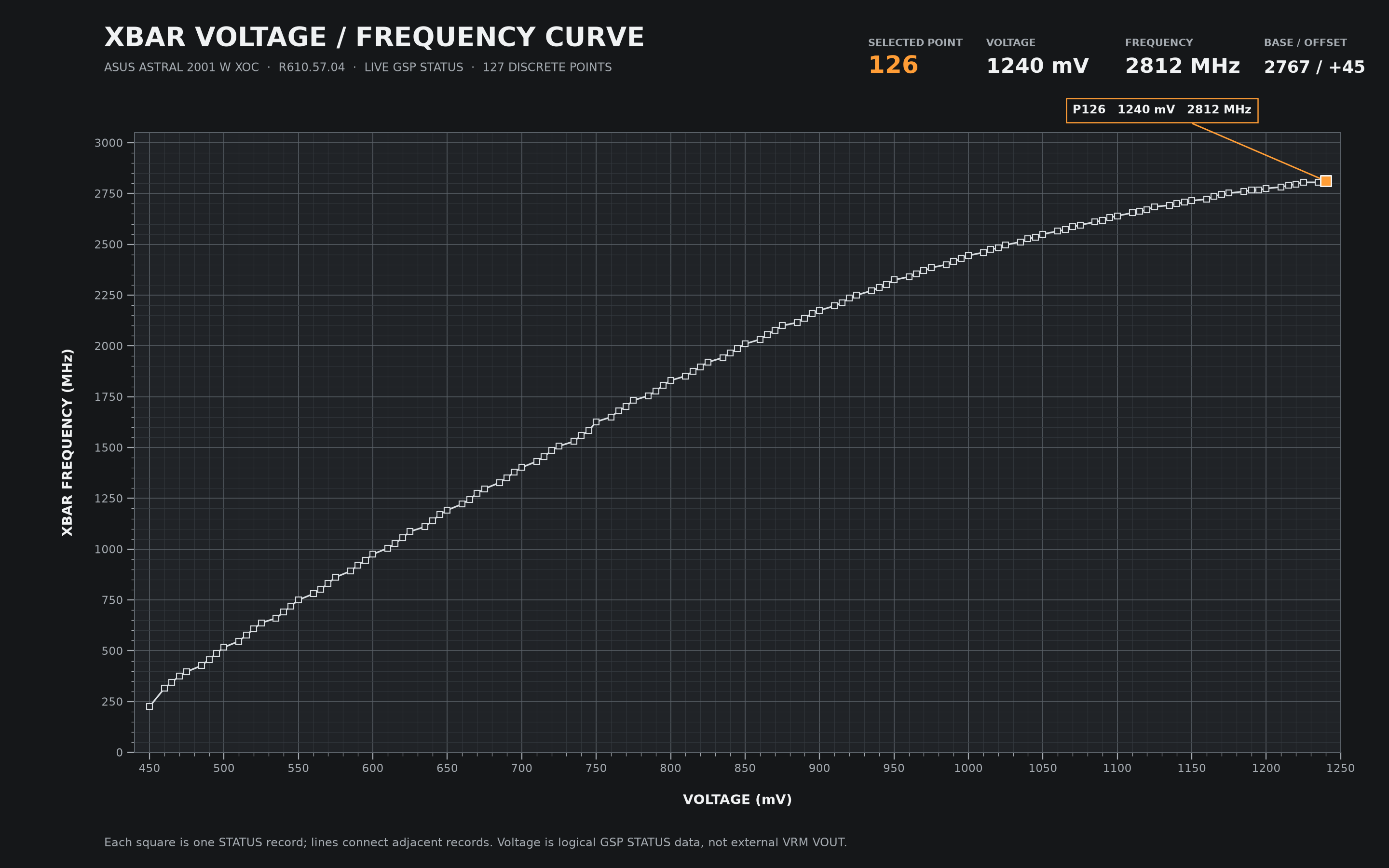
The active Astral 2001 W XOC image was version 98.02.2E.80.50 under R610.57.04. Its read-only NV2080_CTRL_CMD_CLK_VF_POINTS_GET_STATUS capture contains exactly 127 XBAR records. Every record has a +45 MHz tuning term, and every effective frequency equals the decoded base frequency plus 45 MHz.
Offline comparison also found that Astral 2001 W XOC and Lightning 2500 W XOC have byte-identical PERFORMANCE, BOOST, Clock Programming, Voltage Map v0x30, NAFLL, Frequency Controller, Base Clock, Voltage Device, Voltage Rail, and Voltage Policy inputs. Their relevant static curve-input difference is FactoryOC: +45 MHz / 2580 MHz versus +195 MHz / 2730 MHz. Holding the GPU, driver, temperature, fuse/speedo inputs, and generator behavior constant therefore gives a controlled Lightning projection exactly 150 MHz above the captured Astral curve. The projected endpoint is 1240 mV / 2962 MHz; it is not a Lightning live capture and says nothing by itself about delivered voltage or stability.
The curve below follows the presentation of a desktop V/F curve editor: every live record is a discrete square node connected to its neighbours, voltage is horizontal, and effective frequency is vertical. It plots only the measured Astral STATUS bank; the Lightning result remains an explicitly conditional projection rather than being drawn as if it had been captured.
Complete 127-point STATUS table
Collapsed by default. Values are reproduced from the downloadable raw CSV.
| Point | STATUS voltage (mV) | Base frequency (MHz) | Tuning offset (MHz) | Effective frequency (MHz) |
|---|---|---|---|---|
| 0 | 450 | 180 | +45 | 225 |
| 1 | 460 | 270 | +45 | 315 |
| 2 | 465 | 300 | +45 | 345 |
| 3 | 470 | 330 | +45 | 375 |
| 4 | 475 | 352 | +45 | 397 |
| 5 | 485 | 382 | +45 | 427 |
| 6 | 490 | 412 | +45 | 457 |
| 7 | 495 | 442 | +45 | 487 |
| 8 | 500 | 472 | +45 | 517 |
| 9 | 510 | 502 | +45 | 547 |
| 10 | 515 | 532 | +45 | 577 |
| 11 | 520 | 562 | +45 | 607 |
| 12 | 525 | 592 | +45 | 637 |
| 13 | 535 | 615 | +45 | 660 |
| 14 | 540 | 645 | +45 | 690 |
| 15 | 545 | 675 | +45 | 720 |
| 16 | 550 | 705 | +45 | 750 |
| 17 | 560 | 735 | +45 | 780 |
| 18 | 565 | 757 | +45 | 802 |
| 19 | 570 | 787 | +45 | 832 |
| 20 | 575 | 817 | +45 | 862 |
| 21 | 585 | 847 | +45 | 892 |
| 22 | 590 | 877 | +45 | 922 |
| 23 | 595 | 900 | +45 | 945 |
| 24 | 600 | 930 | +45 | 975 |
| 25 | 610 | 960 | +45 | 1005 |
| 26 | 615 | 982 | +45 | 1027 |
| 27 | 620 | 1012 | +45 | 1057 |
| 28 | 625 | 1042 | +45 | 1087 |
| 29 | 635 | 1065 | +45 | 1110 |
| 30 | 640 | 1095 | +45 | 1140 |
| 31 | 645 | 1125 | +45 | 1170 |
| 32 | 650 | 1147 | +45 | 1192 |
| 33 | 660 | 1177 | +45 | 1222 |
| 34 | 665 | 1200 | +45 | 1245 |
| 35 | 670 | 1230 | +45 | 1275 |
| 36 | 675 | 1252 | +45 | 1297 |
| 37 | 685 | 1282 | +45 | 1327 |
| 38 | 690 | 1305 | +45 | 1350 |
| 39 | 695 | 1335 | +45 | 1380 |
| 40 | 700 | 1357 | +45 | 1402 |
| 41 | 710 | 1387 | +45 | 1432 |
| 42 | 715 | 1410 | +45 | 1455 |
| 43 | 720 | 1440 | +45 | 1485 |
| 44 | 725 | 1462 | +45 | 1507 |
| 45 | 735 | 1485 | +45 | 1530 |
| 46 | 740 | 1515 | +45 | 1560 |
| 47 | 745 | 1537 | +45 | 1582 |
| 48 | 750 | 1582 | +45 | 1627 |
| 49 | 760 | 1605 | +45 | 1650 |
| 50 | 765 | 1635 | +45 | 1680 |
| 51 | 770 | 1657 | +45 | 1702 |
| 52 | 775 | 1687 | +45 | 1732 |
| 53 | 785 | 1710 | +45 | 1755 |
| 54 | 790 | 1732 | +45 | 1777 |
| 55 | 795 | 1762 | +45 | 1807 |
| 56 | 800 | 1785 | +45 | 1830 |
| 57 | 810 | 1807 | +45 | 1852 |
| 58 | 815 | 1830 | +45 | 1875 |
| 59 | 820 | 1852 | +45 | 1897 |
| 60 | 825 | 1875 | +45 | 1920 |
| 61 | 835 | 1897 | +45 | 1942 |
| 62 | 840 | 1920 | +45 | 1965 |
| 63 | 845 | 1942 | +45 | 1987 |
| 64 | 850 | 1965 | +45 | 2010 |
| 65 | 860 | 1987 | +45 | 2032 |
| 66 | 865 | 2010 | +45 | 2055 |
| 67 | 870 | 2032 | +45 | 2077 |
| 68 | 875 | 2055 | +45 | 2100 |
| 69 | 885 | 2070 | +45 | 2115 |
| 70 | 890 | 2092 | +45 | 2137 |
| 71 | 895 | 2115 | +45 | 2160 |
| 72 | 900 | 2130 | +45 | 2175 |
| 73 | 910 | 2152 | +45 | 2197 |
| 74 | 915 | 2167 | +45 | 2212 |
| 75 | 920 | 2190 | +45 | 2235 |
| 76 | 925 | 2205 | +45 | 2250 |
| 77 | 935 | 2227 | +45 | 2272 |
| 78 | 940 | 2242 | +45 | 2287 |
| 79 | 945 | 2257 | +45 | 2302 |
| 80 | 950 | 2280 | +45 | 2325 |
| 81 | 960 | 2295 | +45 | 2340 |
| 82 | 965 | 2310 | +45 | 2355 |
| 83 | 970 | 2325 | +45 | 2370 |
| 84 | 975 | 2340 | +45 | 2385 |
| 85 | 985 | 2355 | +45 | 2400 |
| 86 | 990 | 2370 | +45 | 2415 |
| 87 | 995 | 2385 | +45 | 2430 |
| 88 | 1000 | 2400 | +45 | 2445 |
| 89 | 1010 | 2415 | +45 | 2460 |
| 90 | 1015 | 2430 | +45 | 2475 |
| 91 | 1020 | 2437 | +45 | 2482 |
| 92 | 1025 | 2452 | +45 | 2497 |
| 93 | 1035 | 2467 | +45 | 2512 |
| 94 | 1040 | 2482 | +45 | 2527 |
| 95 | 1045 | 2490 | +45 | 2535 |
| 96 | 1050 | 2505 | +45 | 2550 |
| 97 | 1060 | 2520 | +45 | 2565 |
| 98 | 1065 | 2527 | +45 | 2572 |
| 99 | 1070 | 2542 | +45 | 2587 |
| 100 | 1075 | 2550 | +45 | 2595 |
| 101 | 1085 | 2565 | +45 | 2610 |
| 102 | 1090 | 2572 | +45 | 2617 |
| 103 | 1095 | 2587 | +45 | 2632 |
| 104 | 1100 | 2595 | +45 | 2640 |
| 105 | 1110 | 2610 | +45 | 2655 |
| 106 | 1115 | 2617 | +45 | 2662 |
| 107 | 1120 | 2625 | +45 | 2670 |
| 108 | 1125 | 2640 | +45 | 2685 |
| 109 | 1135 | 2647 | +45 | 2692 |
| 110 | 1140 | 2655 | +45 | 2700 |
| 111 | 1145 | 2662 | +45 | 2707 |
| 112 | 1150 | 2670 | +45 | 2715 |
| 113 | 1160 | 2677 | +45 | 2722 |
| 114 | 1165 | 2692 | +45 | 2737 |
| 115 | 1170 | 2700 | +45 | 2745 |
| 116 | 1175 | 2707 | +45 | 2752 |
| 117 | 1185 | 2715 | +45 | 2760 |
| 118 | 1190 | 2722 | +45 | 2767 |
| 119 | 1195 | 2722 | +45 | 2767 |
| 120 | 1200 | 2730 | +45 | 2775 |
| 121 | 1210 | 2737 | +45 | 2782 |
| 122 | 1215 | 2745 | +45 | 2790 |
| 123 | 1220 | 2752 | +45 | 2797 |
| 124 | 1225 | 2760 | +45 | 2805 |
| 125 | 1235 | 2760 | +45 | 2805 |
| 126 | 1240 | 2767 | +45 | 2812 |
The voltage axis is the effective-voltage field in the GSP STATUS object. It must not be relabelled as externally measured regulator VOUT. The downloadable raw CSV preserves all 127 records, record offsets, the 16.16 base value, source-voltage field, duplicate fields, and both tuning offsets.
What is confirmed and what is not
Confirmed:
- GB202 XBARCLK is an active hardware clock domain separate from GPCCLK, SYSCLK, and MCLK.
- It has an independent PMU object, source ID, apply/commit path, and eventual MMIO-write chain.
- A private hardware counter can measure XBARCLK independently.
- XBAR frequency and domain-voltage requests change its 127-point effective V/F state.
- On R610.57.04, runtime XBAR/MSVDD offset requests read back exactly, change physically measured frequency and rendering throughput, and can be restored.
- The active topology contains a GPC→XBAR ratio relation and rail-1 shared-voltage relations among MCLK, XBAR, and SYS.
- A finite maximum endpoint that does not constrain physical MCLK can still place XBAR/SYS in another hardware and controller state.
- Directly creating the same low-XBAR state is sufficient to reproduce key downstream feedback from the MCLK-MAX state.
- NVIDIA rail status separates current/default, current target, sensed value, and multiple limits. A single HWiNFO
GPU MSVDD Voltagescreenshot is not proof of physical VOUT.
High-confidence inferences:
- Current R610 uses the active type-5 relation to convert a finite MCLK maximum endpoint into a shared-voltage range and propagate it into XBAR/SYS ranges.
- XBARCLK performs the local physical programming, while XBAR2CLK is closer to a logical or policy-aggregation domain.
- The roughly 3% independent game gain comes from improved throughput in an on-chip data path driven by XBARCLK, rather than higher GPC or SYS frequency.
Still unknown:
- Every module, endpoint, and interconnect covered by XBARCLK on the GB202 floorplan.
- The exact private R610 function and live range fields executing type-5 conversion.
- The exact hardware-register offsets populated in the live XBAR source descriptor.
- Whether NVIDIA considers cross-domain propagation from a non-binding MCLK MAX to be intended behavior.
- Whether the direct ClockClient XBAR-frequency path generalizes across GB202 samples, driver branches, and VBIOSes; the forum's multi-sample indirect MSVDD path is not a substitute.
- Whether future drivers preserve the private ClockClient command layout and semantics.
- Which NVIDIA rail-status field HWiNFO maps to
GPU MSVDD Voltageon the cited build and Matrix. HWiNFO is closed-source and no author confirmation has been found; current behavior supports only the conservative statement that it is consistent with logical rail state. - A long-term stable XBAR voltage/frequency boundary.
Conclusion
The important part of XBAR is not how many percent it can add in one short benchmark. It reveals the real shape of a modern GPU control system: a physical clock domain almost invisible in public interfaces can have its own V/F state and hardware-programming path while remaining closed-loop coupled to core, memory, and SYS through clock propagation, a shared voltage rail, and power estimation. Every software request is only an input to that constraint network; final hardware state depends on which constraint becomes active.
The MCLK-MAX anomaly supplied a strong enough experimental perturbation to turn that hidden path from a telemetry correlation into a causal chain that can be controlled, reproduced, and tested in reverse. It also demonstrates that the most valuable result in private driver and firmware research is rarely finding an offset that accepts a write. It is proving which hardware path the write traverses, what physical state it changes, and under which conditions a different arbiter overrides it.
Evidence and downloads
The compact download index maps every local research filename cited below to a directly downloadable copy and records its SHA-256. The SHA256SUMS file can be verified after downloading with sha256sum -c SHA256SUMS.
- Runnable R610.57.04 XBAR ClockClient minimal example
- GB202 PMU clock domains, XBAR hardware measurement, and propagation topology
- Finite DRAM-MAX to XBAR/power-feedback closure
- XBAR runtime frequency and domain-voltage control
- XBAR 127-point live V/F state
- Raw Astral 2001 W XOC 127-point STATUS CSV
- Static discrete-node export of the Astral XBAR V/F curve
- FactoryOC values and hashes for 15 representative RTX 5090 VBIOS images
- XBAR-only A–B–A in two games under the normal state
- XBAR 2400 recovery experiment under the MCLK-MAX fault state
- MSI Lightning VBIOS cross-experiment
- NVIDIA #1265: initial memory locked-clock anomaly
- NVIDIA #1266: finite MCLK MAX propagation into XBAR/SYS and fresh reproduction
- LACT #1128: separating a memory offset from a locked-clock range
- LACT #1147: direct XBAR/MSVDD requests and game A–B–A
- Public evidence-package reproduction report
- Raw telemetry and benchmark-output verification
- Overclock.net page 1945: external I²C/MSVDD failure and the “hardware modification required” inference
- Overclock.net page 1947: melonVolt's private NVAPI path and initial reproductions
- Overclock.net page 1949: multi-card XBAR gains, saturation, and black screens
- Overclock.net page 1950: three-step control, MSVDD saturation, and melonVolt+ECB
- Overclock.net page 1956: XOC VBIOS, the MSVDD ceiling, and EVC2 physical VOUT
- Overclock.net page 1959: rushed melonVolt 0.2a release and risk statement
- Overclock.net page 1960: the 1.15 V screenshot, MSI XOC memory range, and HDMI cross-flash cost
- Overclock.net page 1961: using black-screen threshold as a false daily-safety rule
- HWiNFO official version history: version 8.42 MSI RTX 5090 Lightning VRM monitoring
- Overclock.net current final page as of 2026-08-13
- Read-only text mirror of Overclock.net page 1945
DISCUSSION